Home
› Full Adder Logic Diagram And Truth Table : (a) Full adder logic diagram and (b) its truth table. | Download Scientific Diagram / The truth table is shown.
Full Adder Logic Diagram And Truth Table : (a) Full adder logic diagram and (b) its truth table. | Download Scientific Diagram / The truth table is shown.
Full Adder Logic Diagram And Truth Table : (a) Full adder logic diagram and (b) its truth table. | Download Scientific Diagram / The truth table is shown.. The c out will only be though the implementation of larger logic diagrams is possible with the above full adder logic, a simpler symbol is mostly used to represent the operation. It can be used in many applications like, encoder, decoder, bcd after making the connection verify the full adder truth table. In the above image, instead of block diagram, actual symbols are shown. Full adder using nor logic: Half adder and full adder.
For example, consider the case a = 1, b = 0 and c = 1. Which is add a 3 bit data and generate output carry and sum. An adder is a device that can add two binary digits. A, b and cin, which add three input binary digits and generate two binary outputs i.e. Draw the logic diagram for a circuit that implements the function in question 7.
Half Adder Logic Diagram And Truth Table - Wiring Diagram Schemas from circuitdigest.com **draw truth table and logic diagram of full subtractor.** the full subtractor is a combinational circuit with three inputs a, b and bin and two outputs d and bo. Truth table is a representation of a logical expression in tabular format. The c out will only be though the implementation of larger logic diagrams is possible with the above full adder logic, a simpler symbol is mostly used to represent the operation. The full adder circuit diagram add three binary bits and gives result as sum, carry out. Full adder is a combinational device. Each output generated can be expressed in terms of boolean function. Express sum and carry in terms of mean terms and max terms. The logic gates present in it acts based upon the signals.
In these circuits there are n input variables obtained from an external source are of binary type.
Draw the logic diagram for a circuit that implements the function in question 7. Full adder is the adder which adds three inputs and produces two outputs. This tool helps you solve and get results of boolean expressions with logic symbols quickly. Truth table with three inputs. Full adder using nor logic: Which is add a 3 bit data and generate output carry and sum. An adder is a device that can add two binary digits. The full adder (abbreviated fa) must add these bits to produce a sum of 0 and a carry out of 1. F = 1 if and only if there is a 0 to the left of a 1 in the input. When led glows it represents logic high (1), during off condition led represents logic. Each output generated can be expressed in terms of boolean function. Even though this is a simple adder and can be used to add unrestricted bit length numbers, it is however not very efficient. Full adder definition, block diagram, truth table, circuit diagram, logic diagram, boolean expression and equation are discussed.
In the above image, instead of block diagram, actual symbols are shown. Truth table is a representation of a logical expression in tabular format. Full adder working principle circuit diagram etc. **draw truth table and logic diagram of full subtractor.** the full subtractor is a combinational circuit with three inputs a, b and bin and two outputs d and bo. Which is add a 3 bit data and generate output carry and sum.
Half Adder, Full Adder, Half Subtractor & Full Subtractor from i0.wp.com In the above image, instead of block diagram, actual symbols are shown. Full adder i truth table logic diagram eeeguide com. One is half adder and another one is known as full adder. Express sum and carry in terms of mean terms and max terms. Full adder is a combinational device. When led glows it represents logic high (1), during off condition led represents logic. **draw truth table and logic diagram of full subtractor.** the full subtractor is a combinational circuit with three inputs a, b and bin and two outputs d and bo. Adders are classified into two types:
The full adder (abbreviated fa) must add these bits to produce a sum of 0 and a carry out of 1.
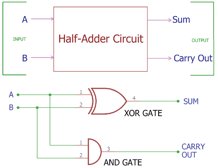
When a logic gate has only two inputs, or the logic circuit to be analyzed has only one or two gates, it is fairly easy to remember how a. We can see that the output s is an exor between the input a and the. • three inputs x, y, and z; The sum 's' is produced in two steps the implementation of larger logic diagrams is possible with the above full adder logic a simpler symbol is mostly used to represent the operation. **draw truth table and logic diagram of full subtractor.** the full subtractor is a combinational circuit with three inputs a, b and bin and two outputs d and bo. Half adder and full adder. The output s is an xor between the input a and the half adder sum output with b and c in inputs. This can be implemented using and, or and not gates as shown below. The block diagram is shown. An adder is a digital logic circuit in electronics that performs the operation of additions of two number. Full adder circuit construction is shown in the above block diagram, where two half adder circuits added together with a or gate. Truth tables offer a simple and easy to understand tool that can be used to determine the output of any logic gate or circuit for all input combinations. Full adder combinational logic circuits electronics tutorial.
The truth table is shown. This can be implemented using and, or and not gates as shown below. The full adder (abbreviated fa) must add these bits to produce a sum of 0 and a carry out of 1. When a logic gate has only two inputs, or the logic circuit to be analyzed has only one or two gates, it is fairly easy to remember how a. Create truth tables with this free truth table generator online.
Adders and Subtractors | Digital Circuits 3: Combinational Circuits | Adafruit Learning System from cdn-learn.adafruit.com In order to arrive at the logic logic circuit diagram of full adder. Full adder working principle circuit diagram etc. Diagram using basic logic gates. For example, consider the case a = 1, b = 0 and c = 1. Full adder using nor logic: Half adder and full adder. Full adder i truth table logic diagram eeeguide com. The truth table and corresponding karnaugh maps for it.
It is a type of digital circuit that performs the operation of additions of two number.
This tool generates truth tables for propositional logic formulas. An adder is a device that can add two binary digits. In these circuits there are n input variables obtained from an external source are of binary type. Figure shows the truth table of a full adder circuit showing all possible input combinations and corresponding outputs. I drew the truth i think v hav to use full adder here.is tht? Draw the truth table for a logic function that takes a three bit binary number and produced an output that is 0 for even parity and 1 for odd parity. It is mostly used in mathematics and computer science. • three inputs x, y, and z; Draw the logic diagram for a circuit that implements the function in question 7. It can be used in many applications like, encoder, decoder, bcd after making the connection verify the full adder truth table. Express sum and carry in terms of mean terms and max terms. There are eight possible cases for three inputs and for each case the desired output values are listed. Full adder i truth table logic diagram eeeguide com.